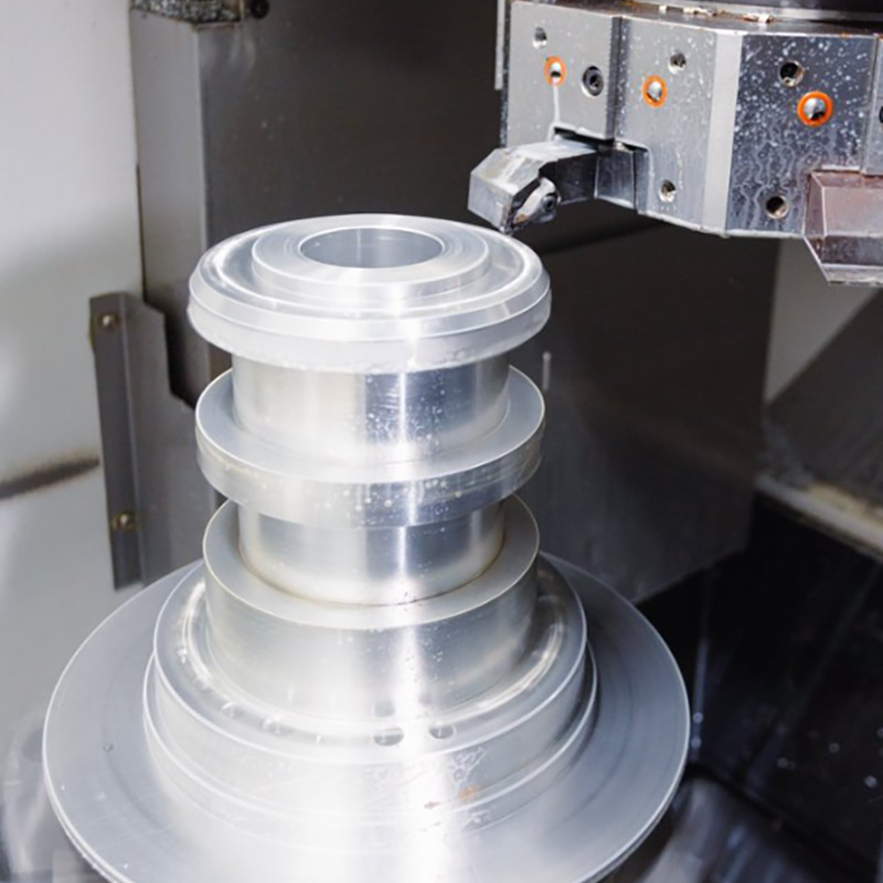
Semiconductor equipment operates in some of the most demanding manufacturing environments on earth—clean room conditions, ultra-high vacuum or precisely controlled atmospheric pressures, aggressive chemical exposure, and thermal cycling that would destroy conventional engineering components. Machined parts for semiconductor equipment must meet dimensional tolerances that are often measured in microns, surface finish requirements specified in nanometers, and material cleanliness standards that minimize contamination risk for the wafers and devices being processed.
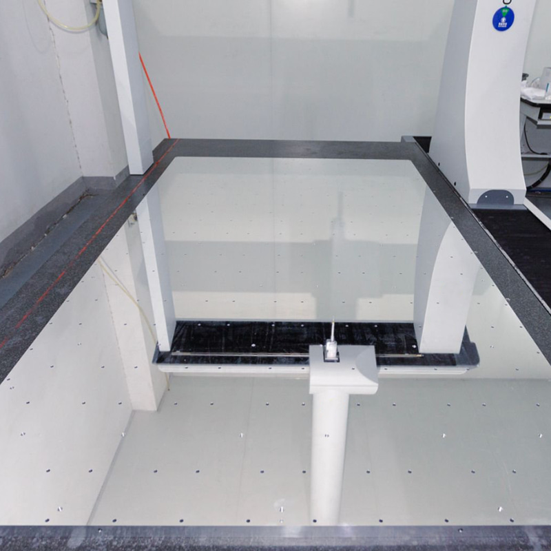
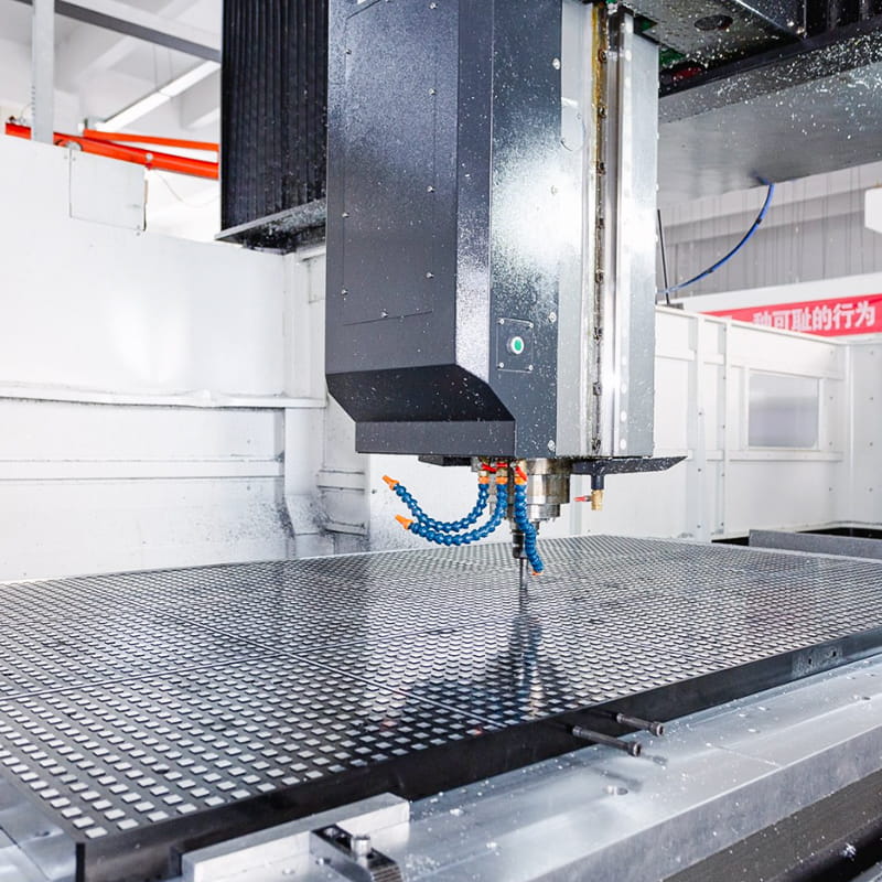
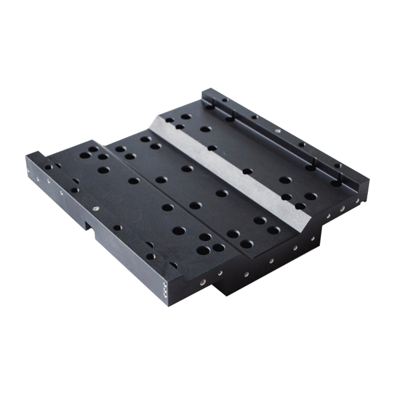
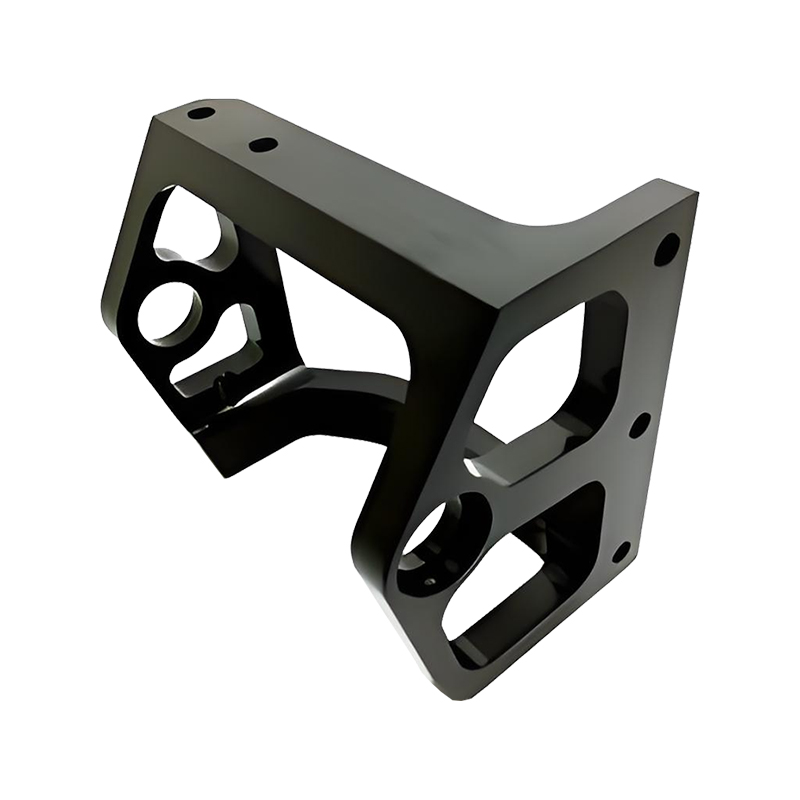
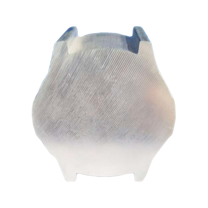
Our semiconductor equipment machined components are primarily focused on wafer dicing stage platforms and supporting structures. Wafer dicing stages require extreme flatness across the full vacuum chuck surface (typically better than 2 μm total flatness across the working area), bore and channel tolerances compatible with vacuum sealing systems, and surface finishes that support uniform wafer contact without contamination risk. Repeat positioning accuracy of ±1 μm or better is the standard expectation for X/Y motion axes in these systems.
Material selection is carefully matched to the chemical environment. Aluminum alloys are standard for lower-chemical-exposure components; hard anodized 6061 or 6082 provides surface hardness and chemical resistance for moderate-exposure applications. Vacuum compatibility requires attention to outgassing characteristics, surface texture specification, and the elimination of blind holes or trapped-volume features that would affect chamber pump-down performance.
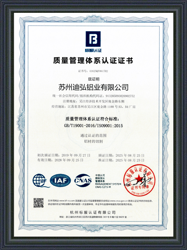
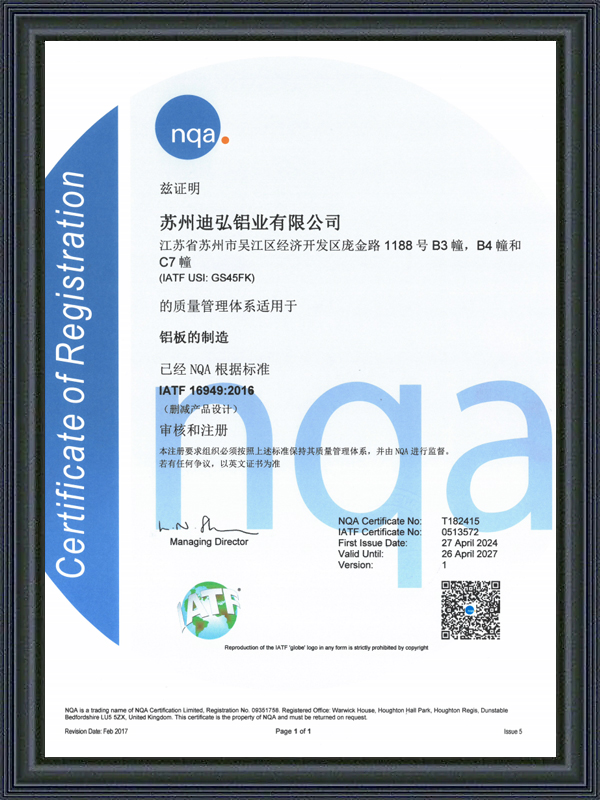
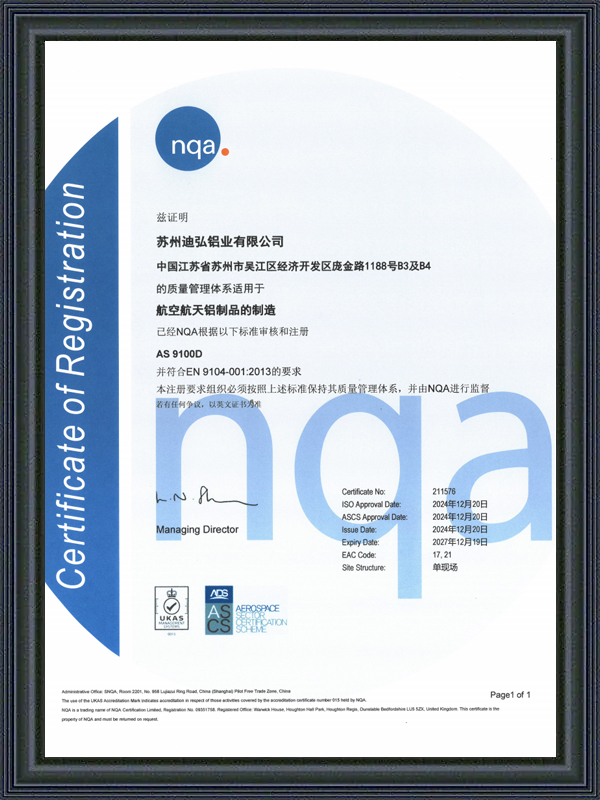
We support full documentation packages for semiconductor equipment qualification, including dimensional inspection reports, material certifications, surface finish records, and cleanliness verification. Machining is conducted in controlled-environment conditions to meet the particulate requirements of the semiconductor manufacturing sector.


 English
 Español
 عربى
عربى